HMC E155 Lab 2: Multiplexed 7-Segment Display
Introduction
In this lab, a state-based solution was created to independently take the inputs of two 4-segment switches (to represent hex numbers) and display them on a two-diget seven segment display using only one seven segment decoder, necessitating an FSM. A switching frequency was generated, and addtionally, the sum of the two switches at any given time was displayed using a string of LEDs in binary representation.
Block Diagram
The block diagram in the below image shows the hierarchical structure of the Verilog modules written for this lab. The top module (lab2_ly) contains all other modules, and the HSOSC module from the UP5K board is used. A counter module was reused from lab 1 to modulate the clock down to ~90 Hz on the 17st bit of the counter, allowing it to oscillate the power between our two sides of the seven segment display, also representing our two states. A single decoder determined the multiplexed selection between the two switch outputs, and a full adder determined the LED binary output.
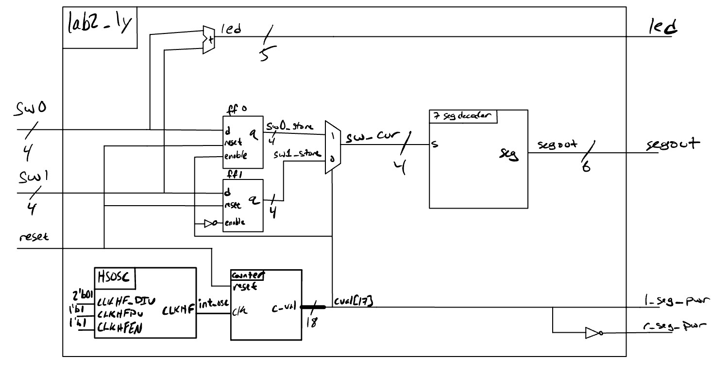 Figure 1: Block diagram of hierarchical SystemVerilog
Schematic
The two schematics below show how the LEDs in the given system are powered. The 7-segment display common power pins are given a ~3.3V input through a PNP transistor with 1 \(\mu A\) at the base (necessitating an ~330 \(\Omega\) resistor), and pins at the end of them are pulled high to turn off a given segment. Only one set of pins was powered and pulled appropriately at any given time, and the 90 Hz oscillating frequency ensured stable powering without blending of the two signals. As per the last lab, a 200 \(\Omega\) resistor was selected as a current limiting resistor. The pins connected to the breakout switch were connected to ground with pullup resistors set on the FPGA pins.
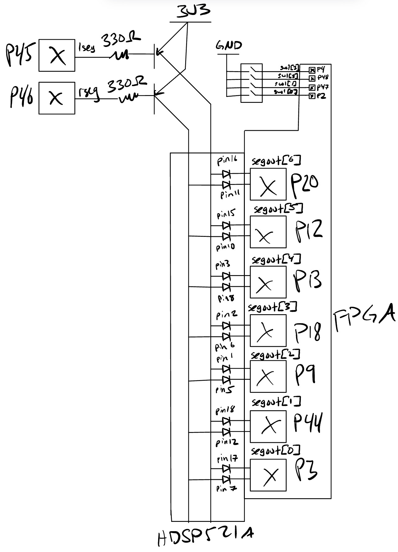 Figure 2: Schematic for the breakout board
Design Testing and Methodology
The onboard oscillator was used from the iCE40 UltraPlus FPGA to generate a clock pulse, which was used with a SystemVerilog counter/clock divider module to control the oscillating LED. The switch banks on the development board and breakout board were used to represent the four binary bits of two hexadecimal numbers, and these switches fed into a full adder to determine when onboard LEDs should be enabled. A state machine toggled between the two switch inputs into the decoder, powering the relevant side of the seven segment display in the process All current-limiting resistors for the 7-segment display were determined with a target current of 7 \(\mu A\) and a voltage drop across the LEDs of 1.95 V, leading to a resistance value of ~ 200 \(\Omega\). A 330 \(\Omega\) resistor was used from the enable pins to power into the base of a PNP transistor with a target current of 1 \(\mu A\). This then fed into the seven segment display from a 3V3 feed on the collector, and the transistors with oscillating base inputs swapped power at about 90 Hz.
All modules were tested using automatic Verilog testbenches as shown in the Results and Discussion section.
Results and Discussion
Testbench Results
Newly written modules (enabled FF and top level) were tested using automated verilog testbenches to ensure that all sums were correct in the outputs, that the power pins swapped at the correct frequency, and that the enabled FF worked as intended. See all testbench results below.
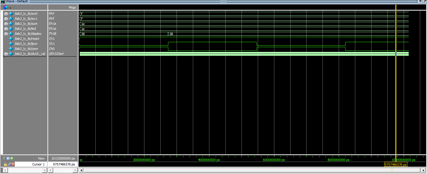 Figure 3: Testbench waveforms showing the oscillating power states on the top module as well as functioning combinational LED logic
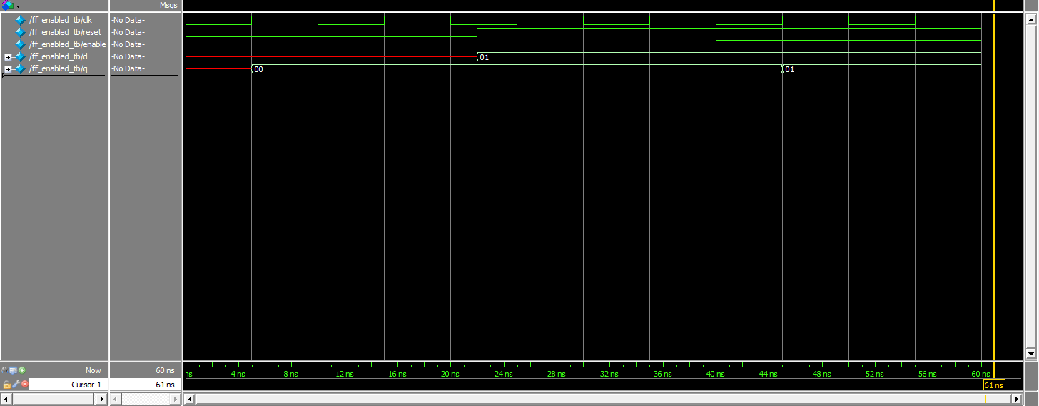 Figure 4: Testbench results showing no errors when testing the counter
7-Segment, Combinational, and Oscillating LEDs Module
Testing verification was done to confirm that the seven segment and LEDs displayed appropriate outputs based on switched inputs. All segments were equally bright, and there was no blending between the two displays due to coupling between the two inputs.
Conclusion
In this lab, I created a SystemVerilog hierarchy and accompanying breakout board that controlled 5 LEDs using a full adder, and used an oscillating FSM to control two separate seven segment LED displays using one decoder. Overall, I spent 5 hours on this lab.
AI Prototype
Following the directions for the AI Prototype for lab 1, the following prompt was passed into ChatGPT:
Write SystemVerilog HDL to leverage the internal high speed oscillator in the Lattice UP5K FPGA and blink an LED at 2 Hz. Take full advantage of SystemVerilog syntax, for example, using logic instead of wire and reg.
The model handled this shockingly well, and no major errors were found in the code itself. It used a slightly lazy way to create a counter, resetting the counter value every time the correct number of cycles had passed rather than creating a counter that uses a P value and the final bit of an N bit counter (as taught in E85). However, this compiled and worked in the Radiant simulation. However, a minor issue that I did notice was that ChatGPT thought the onboard high speed oscillator operated at 12 MHz, not 48 MHz as it actually operates. When this was pointed out to GPT, it quickly corrected that line.
 Figure 8: Code for the oscillator written by ChatGPT, which has many strange ways to specify bit length but otherwise seems very feasible
Another issue that I noticed is that the bit lengths of many constants were not specified. Knowing how many different examples of counters must be in the model, it makes sense that these things would be issues, but it still is slightly surprising that it was so much of an issue. A lot of them only generated warnings in Radiant, but if the code were to be passed through something like Verilator or another SystemVerilog linting program, it would likely point out a lot of other isues as well.